


| 产品特性:厚金PCB | 加工定制:是 | 品牌:中国超盛 |
| 型号:cspcb2906 | 机械刚性:刚性 | 层数:多层 |
| 基材:铜 | 绝缘材料:有机树脂 | 绝缘层厚度:超厚金大尺寸板 |
| 阻燃特性:VO板 | 加工工艺:电解箔 | 增强材料:玻纤布基 |
| 绝缘树脂:环氧树脂(EP) | 产品性质:*** | 营销方式:厂家直销 |
| 营销价格:*** |
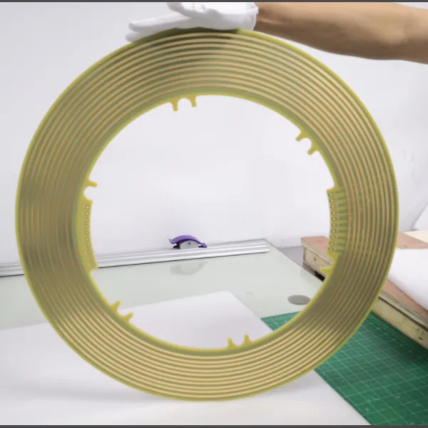
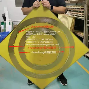
12层,FR-4,TG170,线圈,内层铜2OZ,外层铜3OZ,电镍200um,电金钴金1.5UM(60U“)
厚金大尺寸电感电路板PCB,大尺寸线圈电路板,定制大尺寸PCB,线圈板大尺寸PCB,电感线圈大尺寸PCB,
多层大尺寸线圈PCB,超厚大尺寸PCB,18mm超厚大尺寸PCB,10mm超厚PCB,32层大尺寸PCB,64层大尺寸PCB
,60层大尺寸柔性FPC,超大尺寸软硬结合柔性FPC,大尺寸软硬结合FPC,多层大尺寸柔性FPC,大尺寸柔性FPC,超长
尺寸柔性FPC,双层卷对卷柔性FPC
厚金大尺寸电感电路板(PCB)在现代电子设备中扮演着至关重要的角色,尤其是在高频、高功率的应用场景中。由于其独特的设计和材料特性,厚金电感电路板能够有效降低电阻和损耗,从而提高整体电路的性能和稳定性。大尺寸线圈电路板的应用范围广泛,包括电源管理、无线充电、射频识别(RFID)以及电动汽车的驱动系统等。 在设计厚金大尺寸电感电路板时,制造商需要考虑多个因素,包括电感值、工作频率、温度特性以及电流承载能力等。为了确保电路板的可靠性和长期稳定性,采用高导电性材料和***的制造工艺是至关重要的。此外,合理的布局和走线设计可以减少电磁干扰,提高电路的整体效率。随着技术的不断进步,厚金大尺寸电感电路板的制造成本也逐渐降低,这使得其在市场上的应用愈发广泛。 展望未来,随着5G技术的普及和物联网的发展,对高性能电感电路板的需求将持续增长。制造商需要不断创新,提升产品的性能和可靠性,以满足日益严苛的市场需求。同时,环保和可持续发展的理念也将推动电感电路板材料和工艺的升级,促使行业朝着更绿色、更高效的方向发展

Serial Number Project Manufacturing capability
1 Layers Floors 1-80
2 Maximum size of PCB 2500*1150mm
3 Maximum size of flexible FPC 500mm*100m
4 Maximum size of PCBA 1600mm*1000mm
5 FPCBA maximum size 500mm*100m
6 PCB finished product thickness 0.15-12.0mm
7 Thickness of flexible FPC finished product 0.05-0.60mm
8 Finished copper thickness 12um-1075um
9 Minimum finished aperture of laser hole 0.075mm
10 Minimum line width and spacing 1.5mi/1.50mil
11 Minimum finished hole diameter for through-hole 0.15mm
12 Thickness stacking aspect ratio 1:35
13 By processing methods VIA blind buried hole treatment: ink plug hole, resin plug hole, copper paste plug hole, VCP copper filling hole, silver paste plug hole, carbon oil plug hole, etc
14 Surface Treatment Sinking gold, electroplating nickel gold, electroplating thick gold, electroplating gold+OSP, electroplating nickel gold+sinking gold, electroplating nickel gold+sinking gold+OSP, electroplating gold+OSP, electroplating gold+gold fingers, OSP+gold fingers, lead-free tin spraying, lead-free tin spraying+sinking gold, lead-free tin spraying+gold fingers, lead tin spraying, OSP, sinking tin, sinking silver, electroplating silver
15 Main substrate brands Rogers, Arlon, Taconic, TP-2, Megtron, Neclo, ***la, F4B, 3M, Mitsui Group (Japan Mitsui/Mitsui Top), Taiyo TUC, Taiguang EMC, Tenghui VT, Shengyi SY, Lianmao ITEQ, South Asia NOUYA, DuPont Kappon, Taihong, Hongren Hongren, Xin Yang, Nippon Steel Nippon Stee, Teflon, Yasen, Matsushita, RCC, Mitsui Mitsui Group (Japan Mitsui Top), 3M (USA) 3M Location, Kyocera CERADIR, Jiuhe, Jiuhao, China Porcelain, Huaqing, Ai Shengda, Slitton, Kai Changde, Tongxin, Bergs, Yalong, Taiconieta, etc
16 Solder mask color Green, black, red, yellow, white, blue, purple, matte green, matte black, etc
17 Test service AOI、X-Ray、 Voltage withstand test, short circuit test, soldering test, thermal shock test, functional test, high temperature and high humidity test, first piece tester, etc
18 Molding method CNC shape, punch shape, V-CUT+forming method
19 Finished product warpage ≤0.5%
20 Mechanical aperture tolerance ≤0.025mm
21 Finished product warpage ≤0.5%
22 MiNiLED Minimum PAD 0.065mm/0.065mm
23 Thermal conductivity ≧8W
24 Highest withstand voltage 2500Pa
25 High carbon resistance value and tolerance ≧100→15000Ω±20%
26 Impedance tolerance ≤5→8%Ω
27 IC Carrier Board Series Minimum line width and spacing of 20um/20um
FAQ
Question Point Answer
Q: What information is required for PCB CEGSATE: Gberber files for PCB production, product process instructions, such as material requirements, surface treatment requirements, finished product thickness requirements, PCB stack structure diagram for advanced products, copper thickness requirements for each layer, sample quantity requirements, batch order requirements, product application fields, and other related information are required
Q: What information does PCBA need to provide CEGSATE: BOM report is required (including the brand, specifications, and model of the components), X and Y coordinate numbers of PCBA components, and processing requirements: Do we need to purchase the components on our behalf? Or customer supplied components? Do you need software burning? What is the required quantity? What is the monthly demand and other detailed information.
Question: Is my file secure? CEGSATE: Your files are very secure, and we protect intellectual property rights for our clients throughout the entire process. All files provided by the customer will never be shared with any third party.
Q: What is the minimum order quantity? CESGATE: There is no minimum order quantity in POE. We are able to handle small and large batches flexibly.
Q: Do you have any other services? CESGATE: We mainly focus on PCB+FPC production+SMT+assembly PCBA+component procurement services; In addition, we can also provide programming, testing, software burning, wiring, and shell assembly services; And product design, product development, software development
Q: What is your inspection method? How do you control the quality? CESGATE: In order to ensure the quality of PCB and FPC products, flying pin testing is usually used for samples and small batches; The inner circuit undergoes AOI optical inspection, online AOI inspection, and the finished product undergoes *** inspection through E-SET testing rack. The appearance undergoes *** inspection through fully automatic finished product inspection equipment and FQC. PCBA undergoes automatic optical inspection (AOI), BGA part X-Ray *** radiographic inspection, and first article inspection (FAI). PCBA products that require software burning undergo *** full testing through finished product testing rack according to product functional requirements.
。

超盛集团成立于1968年12月,2012年实施股份制改革,公司以高端印制电路板生产为主,集成设计、开发、加工、生产、销售、外贸为一体,1982年成立日本スーパー盛岡奇株式会,2001年成立浙江坤蓥电子科技有限公司、2007年成立深圳市超盛电子科技有限公司、2010年成立深圳市金林新能源有限公司等四家子公司,以及分布在法国、英国、德国、日本、欧洲、香港等国家及地区多处经销商,是中国目前***实力的(日、港、中)合资电路板制造商之一;特色产品包括:HDI(高密度互连)板、高多层、微波高频、厚铜、金属基、软板、陶瓷、软硬结合板等,产品广泛应用于通讯设备、智能系统、新能源、医疗器械、检测系统、航空航天、LED、通信、汽车、家用电子产品等高科技领域,集团年产值超过千亿,印制电路板年产值350亿以上,月产能45万平米。 公司品质方针质量方针: 服务求诚!质量求精!以质量求生存! 质量目标:全员参与,科学管理、客户至上、品质***、******品质 质量承诺: 产品质量***符合顾客标准,如发生产品质量不合格,对客户损失给予必要赔偿;售后服务承诺:对于客户信息反馈给予认真对待,及时回复,积极处理以客为尊我们深信只有用心面对和迎接每个挑战,才能为顾客提供优质的产品和服务。 企业生存之道: 以质量求生存!以信誉求发展!从管理中创***!的品质!的服务!***的价格!树立超盛形象!给我一次机会!还您一个奇迹。 公司企业文化使命: 为世界电子信息产业提供高品质的线路板(PCB、FPC)和及时、满意的服务 愿景: 成长为世界***的线路板服务企业,为客户、员工、社会、投资者创造价值核心价值观 管理原则:诚信、互助,进步、分享. 以客户为中心: 以市场为导向公司继续关注环保和清洁生产,坚持继续发展战略,坚持中国和全球环境会议。我们拥有***环保体系和设施,可以处理废物,减少浪费,减少能源。 秉承“为世界电子信息产业提供高品质的线路板和及时满意的服务,以市场为导向”的核心价值观,为客户、员工、社会、股东创造价值”这一崇高愿景。 我们的宗旨是客户***,交货准时,持续改进,客户满意,提供***的服务和质量。您的满意是我们的追求!欢迎合作的厂商前来我公司指导!我希望你能给我们一个能保贵意见,也希望贵公司能给我们一个长期合作的好机会!
点击查看>| 企业类型 | 股份合作企业 | 注册资本 | 500.00万人民币 |
| 公司注册地址 | 中国广东深圳市龙岗区爱联社区石岗圩路100号 | 统一社会信用代码 | 91440300359776622G |
| 登记机关 | 深圳工商局 | 法定代表人 | 李先生 |
| 公司成立日期 | 2002-01-28 | 营业期限 | 长期有效 |
| 经营范围 | 主要产品类型及结构 无卤素材料、高频材料、高速材料、金属材料、环保线路板、盲埋孔线路板、高导热铝基、热电分离铜基、PDU母排、铁基以及金属基(芯)混压板、埋铜块板、镶嵌铜块板、埋阻埋容板、超薄BT板、陶瓷基板、特氟龙Teflon(PTFE)板、高频混合介质板、高速板、差分阻抗控制板、厚铜板、高低铜板、阶锑厚铜板、镀厚金板,高阶HDI,任意阶(交叉盲埋)Anylayer、双面FPC、多层FPC、HDIFPC、软硬结合、软硬结合HDI、超长超大尺寸板、超厚板、超小尺寸板、集成电路IC、BGA封装基板、特殊厚铜10CM多层等。 主要表面工艺: 沉金、电镍金、沉金+OSP、电镍金+沉金、电镍金+沉金+OSP、电金+OSP、沉金+金手指、OSP+金手指、无铅喷锡、无铅喷锡+沉金、无铅喷锡+金手指、有铅喷锡、OSP、沉锡、沉银 主要材料有: Rogers、Arlon、Taconic、TP-2、Megtron、Neclo、Isola、F4B、台耀TUC、台光EMC、腾辉VT、生益SY、联茂ITEQ、南亚NOUYA、杜邦Kapton、台虹、宏仁、新扬、新日铁、铁氟龙、雅森、日本松下、日本RCC、日本三井、美国3M、贝格斯、雅隆、泰康尼等。 | ||
-
面议
-
面议
-
面议
-
面议
-
面议
-
面议
-
面议
-
面议
-
¥1.80
-
¥3.80
-
面议
-
面议
